SPI FLASH Recovery for XO-1.5: Difference between revisions
(Incorporated details about Dediprog option) |
|||
| (8 intermediate revisions by 3 users not shown) | |||
| Line 1: | Line 1: | ||
<noinclude>[[Category:Hardware]][[Category:Firmware]][[Category:Repair]]</noinclude> |
|||
| ⚫ | |||
| ⚫ | |||
<font color=red>This page could really use some pictures!</font> |
|||
=== Locating the SPI FLASH === |
=== Locating the SPI FLASH === |
||
The SPI FLASH is U23. It is an 8-pin part that is located "northwest" of the chip marked "ene" (The "ene" chip is the Embedded Controller). The SPI FLASH is labeled "winbond" and either "25X80..." or "25Q80...". |
The SPI FLASH is U23. It is an 8-pin part that is located "northwest" of the chip marked "ene" (The "ene" chip is the Embedded Controller). The SPI FLASH is labeled "winbond" and either "25X80..." or "25Q80...". |
||
[[Image:XO1.5_SPI_Flash.png|thumbnail|right|Location of SPI Flash]] |
|||
=== Option 1 - Replacing the SPI FLASH === |
=== Option 1 - Replacing the SPI FLASH === |
||
| Line 21: | Line 23: | ||
==== Preparing the "Programmer" Machine ==== |
==== Preparing the "Programmer" Machine ==== |
||
To use an XO-1.5 as a programmer machine, you must solder a 6-pin (2x3) "header" connector to J3, located on the " |
To use an XO-1.5 as a programmer machine, you must solder a 6-pin (2x3) "header" connector to J3, located on the "top" (facing the LCD) side of the motherboard, below the main display connector. You must also either solder a diode in the D4 position, next to J3, or short the pads. A diode is best, to protect the working machine from accidental power to the other machine. |
||
[[Image:XO-1.5_Motherboard_Top_C1.jpg|thumbnail|Top side of motherboard]] |
|||
The pads for J3 are laid out for a surface-mount style header connector, but I prefer to use a through-hole style header pin block instead. You can tack-solder the through-hole header to the pads, and it is then much easier to remove later, compared to a surface mount header, which is quite challenging to remove. |
The pads for J3 are laid out for a surface-mount style header connector, but I prefer to use a through-hole style header pin block instead. You can tack-solder the through-hole header to the pads, and it is then much easier to remove later, compared to a surface mount header, which is quite challenging to remove. |
||
[[Image:XO1.5_SPI_Ports.png|center|400px]] |
|||
| ⚫ | |||
<center> |
|||
<table border="2px" cellpadding="6px"> |
|||
<tr><td>1</td><td>MISO</td><td>+3.3V</td><td>2</td></tr> |
|||
<tr><td>3</td><td>SCK</td><td>MOSI</td><td>4</td></tr> |
|||
<tr><td>5</td><td>CS#</td><td>GND</td><td>6</td></tr> |
|||
</table> |
|||
</center> |
|||
Notes: |
|||
| ⚫ | |||
# MISO - Master In, Slave Out. MOSI - Master Out, Slave In |
|||
| ⚫ | |||
# Adding a 2k pullup resistor between pin 1 (+3.3V) and pin 2 (MISO) greatly improves the distance over which the programmer can operate, because the VX855 pin (to which this connector pin is attached) has a weak pull-up. |
|||
I got a diode for D4 from an old XO board that had been "parted out". Pretty much any surface-mount diode will do. You could probably attach an axial-lead small signal diode with careful soldering. |
I got a diode for D4 from an old XO board that had been "parted out". Pretty much any surface-mount diode will do. You could probably attach an axial-lead small signal diode with careful soldering. |
||
| Line 36: | Line 56: | ||
''The problems with this technique are obtaining a diode, removing the board from the case, and then attaching keyboard/display or serial to interact with it. But once you have done this, the programmer can be used to recover numerous target machines.'' |
''The problems with this technique are obtaining a diode, removing the board from the case, and then attaching keyboard/display or serial to interact with it. But once you have done this, the programmer can be used to recover numerous target machines.'' |
||
| ⚫ | |||
# MISO |
|||
| ⚫ | |||
# SCK |
|||
# MOSI |
|||
# CS# |
|||
# GND |
|||
| ⚫ | |||
==== Option 2a - Connecting to the Target Machine with a Clip ==== |
==== Option 2a - Connecting to the Target Machine with a Clip ==== |
||
Latest revision as of 22:22, 30 January 2011
This page describes some ways of "debricking" an XO-1.5 that has failed because the SPI FLASH "boot ROM" contains bad data.
Locating the SPI FLASH
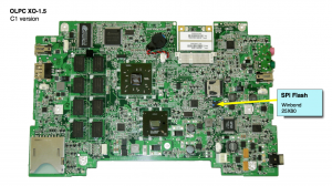
The SPI FLASH is U23. It is an 8-pin part that is located "northwest" of the chip marked "ene" (The "ene" chip is the Embedded Controller). The SPI FLASH is labeled "winbond" and either "25X80..." or "25Q80...".
Option 1 - Replacing the SPI FLASH
If you have soldering equipment and a replacement SPI FLASH part that is programmed with XO-1.5 firmware, you can simply unsolder the old part and replace it with a new one. This might seem like a lot of work, but people with the necessary tools and skill can do it very quickly.
If you aren't highly skilled, Chip Quik ( http://www.chipquikinc.com/ ) can make the job of unsoldering the old part much easier. It is a special alloy that makes solder melt at a much lower temperature, so you can remove the old part with little risk of damaging the board.
The main problem with this "replacement" technique is where to get replacement chips that are already programmed.
Option 2 - Using Another XO-1.5 as a Programmer
The XO-1.5 is designed so that the SPI FLASH part can be programmed "in circuit" without removing the SPI FLASH part. Furthermore, it is also designed so that one (working) XO-1.5 can be used to reprogram another (failed) one.
Preparing the "Programmer" Machine
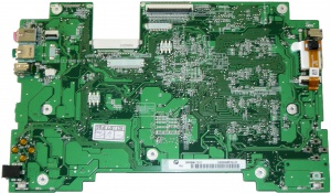
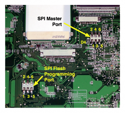
To use an XO-1.5 as a programmer machine, you must solder a 6-pin (2x3) "header" connector to J3, located on the "top" (facing the LCD) side of the motherboard, below the main display connector. You must also either solder a diode in the D4 position, next to J3, or short the pads. A diode is best, to protect the working machine from accidental power to the other machine.
The pads for J3 are laid out for a surface-mount style header connector, but I prefer to use a through-hole style header pin block instead. You can tack-solder the through-hole header to the pads, and it is then much easier to remove later, compared to a surface mount header, which is quite challenging to remove.
The pinout of J3 (and J2) is (top view):
| 1 | MISO | +3.3V | 2 |
| 3 | SCK | MOSI | 4 |
| 5 | CS# | GND | 6 |
Notes:
- +3.3V supplied through the D4 position (diode or shorted)
- MISO - Master In, Slave Out. MOSI - Master Out, Slave In
- Pin 1 is marked with a white dot on the board. The pins are numbered 1,3,5 on the bottom row and 2,4,6 on the top row.
- Adding a 2k pullup resistor between pin 1 (+3.3V) and pin 2 (MISO) greatly improves the distance over which the programmer can operate, because the VX855 pin (to which this connector pin is attached) has a weak pull-up.
I got a diode for D4 from an old XO board that had been "parted out". Pretty much any surface-mount diode will do. You could probably attach an axial-lead small signal diode with careful soldering.
Header pins are very common electronic parts and can perhaps be salvaged from some old piece of gear. Here is one source for purchasing them - http://www.sparkfun.com/commerce/product_info.php?products_id=778 . Longer pin blocks can be cut to the 2x3 length.
Once the header has been attached to the programmer machine, the board will no longer fit in the XO case, so you can't interact with it using the normal techniques. There are several possible workarounds for this problem:
- You could connect a serial adapter and talk to the board with a terminal emulator connected to another computer
- You could remove the display from the XO case and attach it to the board outside, propping it up with some objects to lift it above the programming header connector and its attached cable - and you will also need to either remove the keyboard from the XO case or find some way to move the case close enough to the board so the keyboard cable will reach.
- You could cut a hole in the XO plastic case to make room for the header, and also cut down the header pins to make them shorter (requires a surface mount header).
The problems with this technique are obtaining a diode, removing the board from the case, and then attaching keyboard/display or serial to interact with it. But once you have done this, the programmer can be used to recover numerous target machines.
Option 2a - Connecting to the Target Machine with a Clip
You can clip directly onto the SPI FLASH on the target (failed) machine. You need a clip like this: http://www.hmcelectronics.com/cgi-bin/scripts/product/7420-0001/Pomona-5250/
You also need some wires to connect the clip to the header on the programmer: http://www.sparkfun.com/commerce/product_info.php?products_id=9389
Here is a source for the clip plus wires: http://www.dediprog.com/SPI-flash-accessories/SO8-testclip
The pinout of the SPI FLASH chip is:
- CE# (connect to CS# on programmer)
- SO (connect to MISO on programmer)
- WP# (leave unconnected)
- GND (connect to GND on programmer)
- SI (connect to MOSI on programmer)
- SCK (connect to SCK on programmer)
- HOLD# (leave unconnected)
- VDD (connect to 3.3V on programmer)
Pin 1 is marked with a dot on one corner of the package (it happens to be the upper right corner, since the part is upside-down with respect to the board orientation). From pin 1, the pins are numbered in sequence counterclockwise around the chip.
Option 2b - Connecting to the Target Machine with a Header
Instead of using a test clip, you could solder a 2x3 pin header block to J2 on the target board (after removing it from the case). As with J3, it will be much easier to remove the header later if you tack-solder a through-hole header block to the pads instead of using a surface-mount header block.
With a header block thus attached, you can use a ribbon cable to connect J3 on the programmer to J2 on the target. Premade 6-pin (2x3) ribbon cables are not commonly available, but you can use a larger cable, making sure to connect the corresponding parts of the two ends. Just plug in the cable so pin 1 is next to the marker dot on both ends. (Or you could make a cable that is just the right size by buying two of these http://search.digikey.com/scripts/DkSearch/dksus.dll?Detail&name=609-2841-ND and attaching them to a ribbon cable).
The advantage of the header technique is that the connection is very solid and the cable is simple and reliable. The disadvantage is that you have to remove the board from the case and solder on a connector - and unsolder it later.
Performing the Reflash
Once you have chosen a connection technique, here are the steps for actually doing the reflash.
- DISCONNECT ALL POWER FROM THE TARGET MACHINE!!! Unplug the AC adapter and remove the battery.
- Connect the cable from programmer machine to the target using either the clip technique or the header technique
- Turn on the programmer machine and get to the ok prompt (type the ESC key during the startup jingle)
- Type "clone" at the ok prompt. That will duplicate the programmer machine's OFW image into the target machine
- Alternatively, if you want to put a different OFW image into the target, put the file onto a USB key, insert it into the programmer machine, and type "recover u:\q3a27.rom" (or whatever is the name of your file).
Option 3 - Using a Commercial SPI Programmer
You can program the SPI FLASH with a commercial programmer like http://www.dediprog.com/SPI-flash-in-circuit-programming/SF100 using this clip http://www.dediprog.com/SPI-flash-in-circuit-programming/ISP-Testclip-SO8 .
(Instead of the clip, the header option 2b could be made to work too, but the pinout does not match the programmer so you would need a scrambled cable instead of a straight-through ribbon cable.)
OLPC Firmware Image File Format
OLPC firmware image files are in raw binary format - each byte in the 1 MB file corresponds directly to a byte in the 1 MB SPI FLASH. However, the bytes in the range 0xe0000 to 0xeffff are all 0xff in the image file. In the SPI FLASH, the 64K block from 0xe0000 to 0xeffff is used for "manufacturing data" - information that identifies the specific unit, including its serial number, keyboard layout, and other information that is inserted when the system is manufactured. It is best not to overwrite that 64K block, otherwise the identification information will be lost.
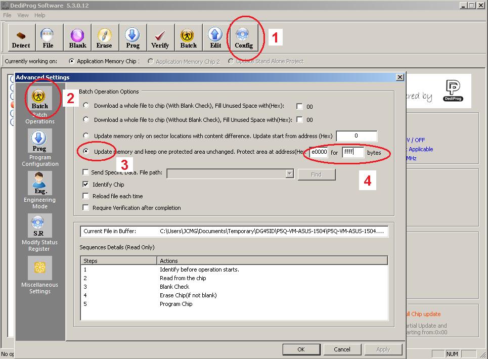
OLPC's reprogramming tools automatically skip that block, programming the ranges from 0x00000 to 0xdffff and 0xf0000 to 0xfffff while leaving the 0xexxxx block alone. To replicate this behavior with the Dediprog programmer, you must do the following, as shown in the illustration below.
- Click on the SF100 "Config' Icon
- Click on the "Batch" Icon
- click on the "update memory and keep one protected area unchanged"
- Define the beginning address "e0000" and the data length "FFFF" to be protected


