XO1.5 1.2V power sequencing ECO: Difference between revisions
No edit summary |
|||
| Line 4: | Line 4: | ||
This only applies to XO-1.5 A-phase (both A1 and A2) motherboards. |
This only applies to XO-1.5 A-phase (both A1 and A2) motherboards. |
||
==Problem Description== |
|||
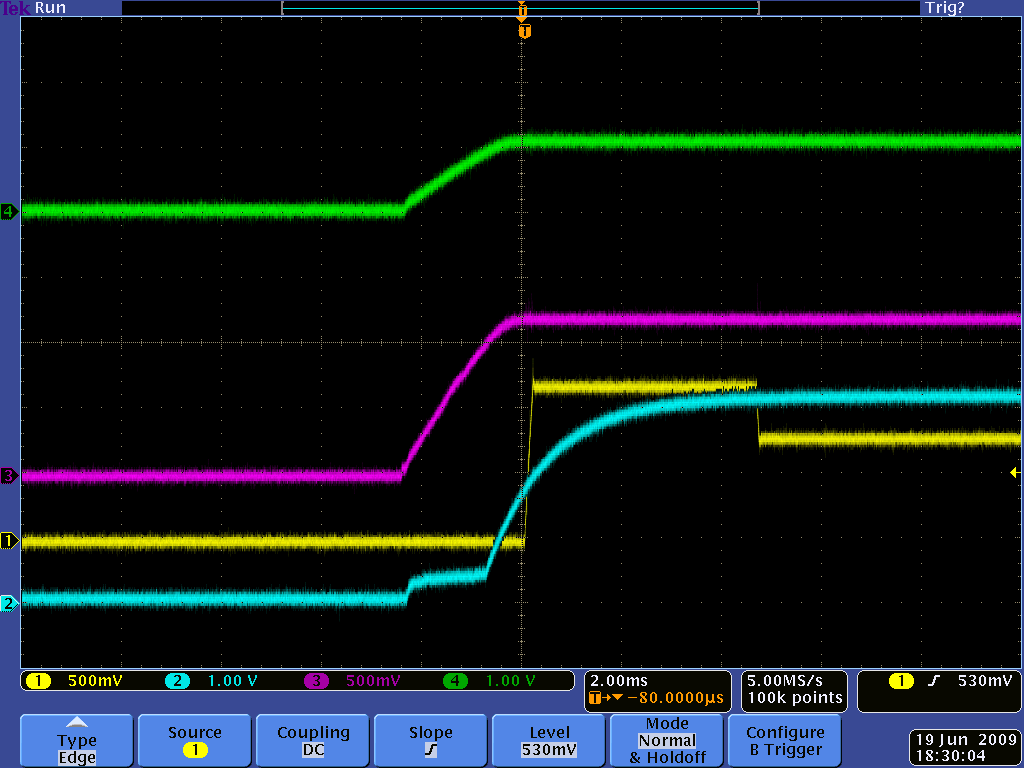
When powering up, the A1 prototypes bring up all run-time power supplies simultaneously, as partially shown in Figure 1: |
|||
[[Image:XO1.5_1.2_Sequence_Powerup.png]] |
|||
* Green - VCCP |
|||
* Magenta - +1.2V |
|||
* Yellow - VCORE |
|||
* Cyan - 1.8V_GOOD (requires +3.3V supply) |
|||
The VX855, while relatively tolerant of run-time power sequencing, does specify that +1.2V (VDD) be supplied before the others. It was possible that other supplies, such as +1.8V and +3.3V, were being supplied to the chip before +1.2V. To correct this, the VX855 SUSB (MAIN_ON) signal is run solely to the +1.2V supply, and the +1.2V_GD (power good) signal is used to drive the MAIN_ON net turning on the remaining supplies. The +1.2V quick drain circuit is disabled by this ECO, the addition of an inverting transistor is required to fix it. |
|||
[[Image:XO1.5_1.2_Sequence_After.png]] |
|||
* Green - VCCP |
|||
* Magenta - 1.8V_GOOD (requires +3.3V supply) |
|||
* Yellow - VCORE |
|||
* Cyan - +1.2V |
|||
=Procedure= |
=Procedure= |
||
Revision as of 00:45, 22 June 2009
Scope
This describes a change to early prototypes of the XO-1.5 motherboard. It fixes a problem with the sequencing of power supply turn-on to the VX855 chip, which prevent power up. Boards having this problem will occasionally fail to turn on, indicated by the EC flashing the red battery charge LED.
This only applies to XO-1.5 A-phase (both A1 and A2) motherboards.
Problem Description
When powering up, the A1 prototypes bring up all run-time power supplies simultaneously, as partially shown in Figure 1:
- Green - VCCP
- Magenta - +1.2V
- Yellow - VCORE
- Cyan - 1.8V_GOOD (requires +3.3V supply)
The VX855, while relatively tolerant of run-time power sequencing, does specify that +1.2V (VDD) be supplied before the others. It was possible that other supplies, such as +1.8V and +3.3V, were being supplied to the chip before +1.2V. To correct this, the VX855 SUSB (MAIN_ON) signal is run solely to the +1.2V supply, and the +1.2V_GD (power good) signal is used to drive the MAIN_ON net turning on the remaining supplies. The +1.2V quick drain circuit is disabled by this ECO, the addition of an inverting transistor is required to fix it.
File:XO1.5 1.2 Sequence After.png
- Green - VCCP
- Magenta - 1.8V_GOOD (requires +3.3V supply)
- Yellow - VCORE
- Cyan - +1.2V
Procedure
- Remove R234 (right next to RTC crystal).
- Lift PU7, pin 6 (near PL6) and tie it to PRE_MAIN_ON (pad of R234 closest to VX855).
- Tie the MAIN_ON (U3, pin 1) signal to +1.2V_GD (D12, cathode).
- Remove PR67 (This is a quick fix. Ideally, pin 2 of PQ20 should be lifted and tied to an inverted, high voltage version of PRE_MAIN_ON).
Results
This page is still a scratchpad testing a hypothesis.
Done to:
- Isabel - which went from frequent red LEDs to never showing one.
