XO1.5 1.2V power sequencing ECO
Scope
This describes a change to early prototypes of the XO-1.5 motherboard. It fixes a problem with the sequencing of power supply turn-on to the VX855 chip, which prevent power up. Boards having this problem will occasionally fail to turn on, indicated by the EC flashing the red battery charge LED.
This only applies to XO-1.5 A-phase (both A1 and A2) motherboards.
Problem Description
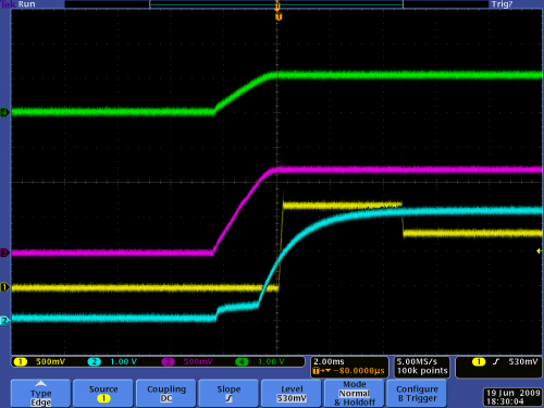
When powering up, the A1 prototypes bring up all run-time power supplies simultaneously, as partially shown in Figure 1:
- Green - VCCP (1.05V supply for processor bus)
- Magenta - +1.2V (VDD supply to VX855)
- Yellow - VCORE (to processor)
- Cyan - 1.8V_GOOD (This signal has a pullup to the +3.3V supply, and shown both the timing to +1.8V being good simultaneous with +1.2V and VCCP, as well as a later turn-on of the +3.3V supply, which enable the VCORE turn-on.)
The VX855, while relatively tolerant of run-time power sequencing, does specify that +1.2V (VDD) be supplied before the others. It is likely that other supplies such as +1.8V and +3.3V are currently supplied to the chip before +1.2V.
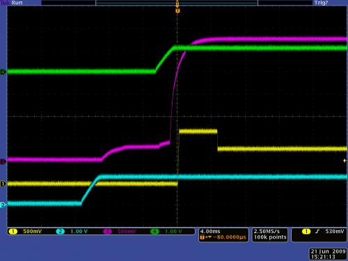
To correct this, the VX855 SUSB (MAIN_ON) signal is run solely to the +1.2V supply, and the +1.2V_GD (power good) signal is used to drive the MAIN_ON net turning on the remaining supplies. The +1.2V quick drain circuit is disabled by this ECO, the addition of an inverting transistor is required to fix it. The resulting timing is shown in Figure 2:
- Green - VCCP
- Magenta - 1.8V_GOOD (requires +3.3V supply)
- Yellow - VCORE
- Cyan - +1.2V (Now happens 8 mS before the others -- we can adjust the +1.2V_GD time constant by removing/changing PC16.)
Procedure
- Remove R234 (right next to RTC crystal).
- Lift PU7, pin 6 (near PL6) and tie it to PRE_MAIN_ON (pad of R234 closest to VX855).
- Tie the MAIN_ON (U3, pin 1) signal to +1.2V_GD (D12, cathode).
- Remove PR67 (near PJP8). This is a quick fix. Ideally, pin 2 of PQ20 should be lifted and tied to an inverted, high voltage version of PRE_MAIN_ON.
Results
This page is still a scratchpad testing a hypothesis.
Done to:
- Isabel - which went from frequent red LEDs to never showing one.

