XO1.5 WLAN ESD protection
Scope
This describes a change to later prototype and early production XO-1.5s. It fixes a problem whereby ESD discharge may damage the internal WLAN module. Laptops without this modification are at risk of becoming inoperable if a static shock is applied at the USB ports, for instance.
This applies to XO-1.5 C1 phase and C2 phase motherboards.
Problem Description
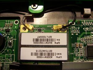
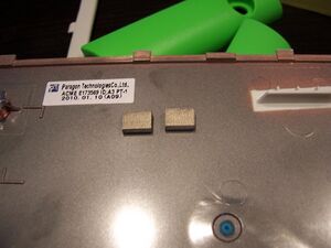
Part of the EMI shielding design for the laptop involves ensuring the sheathing of the WLAN antenna connectors are well grounded. This is accomplished in part by pieces of conductive foam attached to the inside of the laptop's back panel. These pieces of foam connect the metallized coating on the inside of the back panel to the antenna connectors. In some cases the small foam pads are misplaced, and in addition to (or instead of) contacting the antenna connectors, it is centered over a small black IC chip on the WLAN module. If an ESD discharge appears at the USB ports, it will be conducted through the metallized coating, and may "zap" the that IC.
Procedure
- Open the laptop so that the back panel (follow the instructions in Disassembly top) is removed.
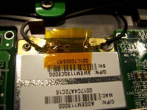
- Apply insulating tape across the exposed chip on the WLAN modules. Leave the antenna connectors uninsulated. The tape should have a dielectric rating of at least 5000V (5kV), such as polymide (also known as Kapton, pictured) or "normal" electrical tape. Using multiple layers is advised.
- In addition, remove the two pieces of foam pictured above. They are not necessary, and are not present on final production laptops.
- Reassemble the laptop.


