XO1.5 WLAN SR ECO: Difference between revisions
| (One intermediate revision by the same user not shown) | |||
| Line 24: | Line 24: | ||
===+3.3V Rise Time=== |
===+3.3V Rise Time=== |
||
Finally, if the rise time of the +3.3V rail isn't fast enough, the card detect debouncer in the SDIO interfaces takes very long (> |
Finally, if the rise time of the +3.3V rail isn't fast enough, the card detect debouncer in the SDIO interfaces takes very long (> 450 mS) to settle on resume. This rise time is determined by a capacitor in the power switch (C253) which needs to be decreased in size. |
||
=Procedure= |
=Procedure= |
||
# Remove R325. R325 and Q38 are located right below the WLAN connector, on the "bottom" side of the PCB (farthest from the LCD). |
|||
# Remove R325. |
|||
# Cut the trace between Q38, pin 2 and R325 (disconnecting Q38, pin 2 from the WLAN_EN# signal). |
# Cut the trace between Q38, pin 2 and R325 (disconnecting Q38, pin 2 from the WLAN_EN# signal). |
||
# Add a 47K resistor between WLAN_EN# (available at R325) and Q38, pin 2. |
# Add a 47K resistor between WLAN_EN# (available at R325) and Q38, pin 2. |
||
# Add a 0.1uF, SMD-0402 resistor between pins 1 and 2 of Q38. |
# Add a 0.1uF, SMD-0402 resistor between pins 1 and 2 of Q38. |
||
# Populate R120 with a 4.7K resistor. |
# Populate R120 with a 4.7K resistor. R120 is located roughly in the middle of the board, on the "top" side. |
||
# Replace C253 with a 0.01 uF SMD0402 capacitor. |
# Replace C253 with a 0.01 uF SMD0402 capacitor. C253 is located above the battery charger and near the EC. |
||
[[Category:Hardware]] |
[[Category:Hardware]] |
||
Latest revision as of 02:32, 25 November 2009
Scope
This describes a change to B3 prototypes of the XO-1.5 motherboard. It fixes a silicon error which will not be fixed. Boards without this ECO will not reliably maintain their WLAN upon resuming, and may crash hard instead.
This only applies to XO-1.5 B3 phase motherboards.
Problem Description
There appear to be three problems: a glitch on the power control line for the WLAN card, a drooping WLAN_RESET# line, and finally, too slow a rise time on the +3.3V rail when resuming.
Power Control Glitch
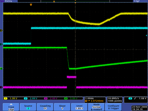
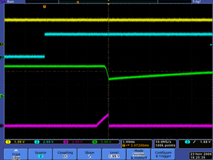
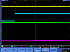
The glitch is a surprise, and is present in both OFW and Linux. It happens early enough in the resume process (before PCIRESET# has been deasserted) that it is caused by hardware. We take a look at it by disconnecting the motherboard pullup resistor on WLAN_EN#, and instead adding a 0.1 uF cap (see Driving Force thumbnail). This transforms the glitch in the WLAN_EN# signal to one which looks like it is driven by a very high impedance driver, such as the built-in pullup resistor.
If we instead add a resistor between the VX855 output and the inverter, along with a filtering capacitor to ground, we can slow down the turn-off process enough that legitimate software usage is allowed, but this glitch is eliminated.
WLAN_RESET
We also need to populate a resistor to pull-up WLAN_RESET# to a sane value. This was predictable, and a resistor position (R120) is pre-wired.
+3.3V Rise Time
Finally, if the rise time of the +3.3V rail isn't fast enough, the card detect debouncer in the SDIO interfaces takes very long (> 450 mS) to settle on resume. This rise time is determined by a capacitor in the power switch (C253) which needs to be decreased in size.
Procedure
- Remove R325. R325 and Q38 are located right below the WLAN connector, on the "bottom" side of the PCB (farthest from the LCD).
- Cut the trace between Q38, pin 2 and R325 (disconnecting Q38, pin 2 from the WLAN_EN# signal).
- Add a 47K resistor between WLAN_EN# (available at R325) and Q38, pin 2.
- Add a 0.1uF, SMD-0402 resistor between pins 1 and 2 of Q38.
- Populate R120 with a 4.7K resistor. R120 is located roughly in the middle of the board, on the "top" side.
- Replace C253 with a 0.01 uF SMD0402 capacitor. C253 is located above the battery charger and near the EC.


