XO 1.5 B3
XO-1.5 Laptop Beta test model 3 (B-Test 3), also known as B3.
Description
The B3 run was motherboards only. If placed in a case, they went into cases with the new (capacitive-only) touchpad. OLPC received fifteen of these in September, 2009. Eventually there were less than ten, and they have been withdrawn, so this page is no longer relevant.
Identification
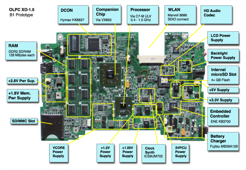
Almost the same as a B2 motherboard:
- The motherboard has a daughtercard for the WLAN.
- The motherboard has an internal SD slot
The noticeable differences are:
- Motherboard revision E
- Only four of eight memory chips populated (512 MB).
- Large polymer (black) capacitors in the processor power supply instead of tantalum (yellow).
- A hole on both sides of the WLAN slot (only on the right in B2).
- Lots of missing small components next to the external SD slot (no support for +1.8V SD slot operation).
Photographs:
Software Support
Firmware
XO-1.5 use Q3xxx firmware releases. These will not work on an XO-1.
Obtaining Firmware
B3 motherboards require a release equal to or later than Q3A15B. There is no current firmware release for B3. Current XO-1.5 firmware releases are not tested on B3.
Upgrading Firmware
See upgrading firmware.
Linux
See release notes.
Hardware Limitations
The currently known hardware problems are:
Lid switch
The lid switch is flaky at best, completely non-operational (lid always closed) at worst. Tracked as #9911. This is fixed in versions of firmware later than Q3A25.
Power Draw
The DC power input on B3s may reach 34W when running firmware earlier than Q3E15. With later firmware, the power draw is still 29W. There is an ECO which restores the laptop power to a 25W limit which should be applied to most B3 motheboards (in time).
WLAN
The WLAN works fine, but requires motherboard ECOs to suspend/resume properly.
Serial Port
The processor serial port situation on XO-1.5 is not optimal, as it shares pins with the camera interface. There is a connector (J4) located on the upper left hand side of the motherboard for +3.3V RS-232 connection (see the pinout and the connector/jumper locations), but its use must be enabled using a jumper or a serial adapter wired correctly (pin 1 tied to GND through a 1K resistor.)
To use the serial port you will have to either short PR148 or short pins 1 and 3 on the SERIAL ENABLE jumper (JP1). PR148 is a large power resistor located near the processor serial port (see the XO-1.5 B2 connector locations). JP1 is located right behind the processor serial port. Be aware that there is a test pad located next to the jumper block that erroneously looks like the pin 1 indicator. Pins 1 and 3 are the two pins closest to the memory chips.
There is no need to disconnect the camera in order to use the serial port. However, any use of the camera while the serial port is enabled will generate constant spurious serial data and is not recommended.
If the SERIAL_ENABLE jumper is set, the camera in-use LED will remain lit. This will not be fixed (Trac ticket #9385).
Documentation
Supporting documentation for these boards are (in PDF):
