B4 Suspend ECR
This page documents a hardware modification to repair a design flaw in the XO-1 B3/B4/C1 laptop motherboards. It is primarily a fix for crashing during suspend/resume (Trac ticket #1835), but includes changes which should improve the reliability of a laptop under all conditions, especially when running from low battery. You are welcome to discuss any experiences on the discussion page.
History
This modification started as a search for the cause of a intermittent USB problem which occurred when reconnecting to the wireless networking interface after a resume. The USB controller was acting in a manner which indicated a hardware problem. A number of developers from Cozybit, AMD, Marvell, RedHat and OLPC worked on the problem for over a month, identifying aggravating conditions and finally reproducing the problem reliably by flood pinging (Trac ticket #1752) --- sending simple "are you there" packets as fast as the network allows --- a machine that was repeatedly suspending and resuming.
Wackup
While testing for this problem, Chris Ball at OLPC was frustrated by another problem (Trac ticket #1835) which appeared while he was trying to reproduce #1752: a crashing of the machine earlier in the resume process. This problem was more unit dependent --- it had never been noticed by other developers working on the problem. Mitch Bradley developed a test in Open Firmware (wackup) which allowed fast and easy reproduction of this earlier crash, using the wireless networking interface to resume the machine a second after it entered suspend.
Using this test, OLPC and Quanta began widespread testing of laptops. It was determined that while some laptops ran for over a hundred thousand suspend/resume cycles before crashing, all did eventually crash. It also discovered that two different crashes were occurring, one where the processor never succeeded in turning off the Microphone LED (the first action on boot, as the microphone power enabling the LED defaults on at power-up), and one where it crashed soon afterwards. The former was labeled 1835a and the latter 1835b.
Clock Stability
Problem 1835a turned out to be a clocking issue: the system clock to the PCI interface on the Southbridge didn't have enough time to stabilize before the on-chip power-good signal was asserted. This problem mainly afflicted systems using a particular clock generator (used in half of the B3s, but not in B4/C build machines), but was present in all laptops. Several different modifications (I, II, III) solve this problem.
Low Battery Problems
In searching for the cause of 1835b, it was noticed that the problems got worse when running from a low battery. This led to the discovery that the switch on the +3.3V line used in suspend/resume was not being properly turned on when the battery was low. This is corrected by changing to a slightly better transistor. At the same time, the target voltage of the WLAN_3.3V supply was increased by 60 mV to insure sufficient voltage after the switch.
Subsystem turn on/off transients
Problem 1835b turned out to be a number of problems, all afflicting the power supplies of the laptop under varying conditions. We had three optional power supplies/switches which were rarely (or never) exercised, but which caused transient dips in critical supplies. These were:
- SD card power - caused a dip in the +3.3V rail
- Camera power - caused a dip in the +3.3V rail
- DCON power - caused a dip in the main memory supply
High Frequency Power Supply Noise
But we still saw a variety of crashes which had been combined into 1835b, the most worrisome were those where the laptop rebooted or powered off, or showed symptoms of memory corruption. Most of these appear to have been due to insufficient high frequency bypassing on different power rails around the laptop. As an example, compare a before and after picture of noise on the +3.3V rail (yellow channel 1) powering the Southbridge USB interface, while the processor accesses the firmware ROM (or keyboard data) over the LPC bus (blue and green channels 2 and 4).
The impact of DCON switching noise on memory stability was seriously tested for several days. Due to their shared power supply, and a large switching transient as the DCON SDRAM interface is powered up, there is a strong possibility for interaction. For example, see this trace, where red (ch 3) is the DCONLOAD signal, blue (ch 2) is the DCON_2.5V supply, and yellow (ch 1) is VMEM. The same trace after bypassing the DCON power supplies shows improvement. Outside of a single failing unit (the reworked one), however, we haven't seen memory corruption on resume.
What's Left ?
With the exception of a laptop with a reworked PCB (new processor), boards modified with the new ECO have performed acceptably. We are still seeing problem with firmware and drivers... And on some laptops, the rebooting continued (Trac ticket #3537), although we have not seen this on any laptop with the full production modification.
Warning
This information is provided in the interest of documenting engineering changes. The changes required by this ECR require advanced surface mount rework skills. There is a good chance that an inexperienced modifier will damage their motherboard. Please take care if you proceed in applying these changes.
A slightly simpler subset of modifications may be made, but they will still require two soldering irons with fine tips and optical magnification of the work area.
C2 Modifications
The final hardware Engineering Change Request to fix the problems encountered on suspend/resume is:
- Tweaking the compensation of the WLAN_3.3V power supply by changing R20 to a 33K resistor (SMD0402, 5%).
- Increasing the voltage of the WLAN_3.3V power supply. There are two common methods:
- Increasing R22 to 32.37K by adding a 768 ohm resistor (SMD0402, 1%) in series to the existing 31.6K resistor
- Decreasing R21 by adding a 330Kohm (SMD0402, 1%) resistor in parallel with the existing 10K resistor
- Delaying the Southbridge reset signal to account for PCI clock stabilitization by:
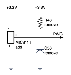
- Installing a 3.10V (3.05 to 3.15V) CPU supervisor, with a delay of at least 16 mS, such as the Micrel MIC811T, driving the PWG signal on the motherboard (1835 ECO II), or
- Installing an RC circuit and buffer to generate the delay (1835 ECO III --- this is the solution for production).
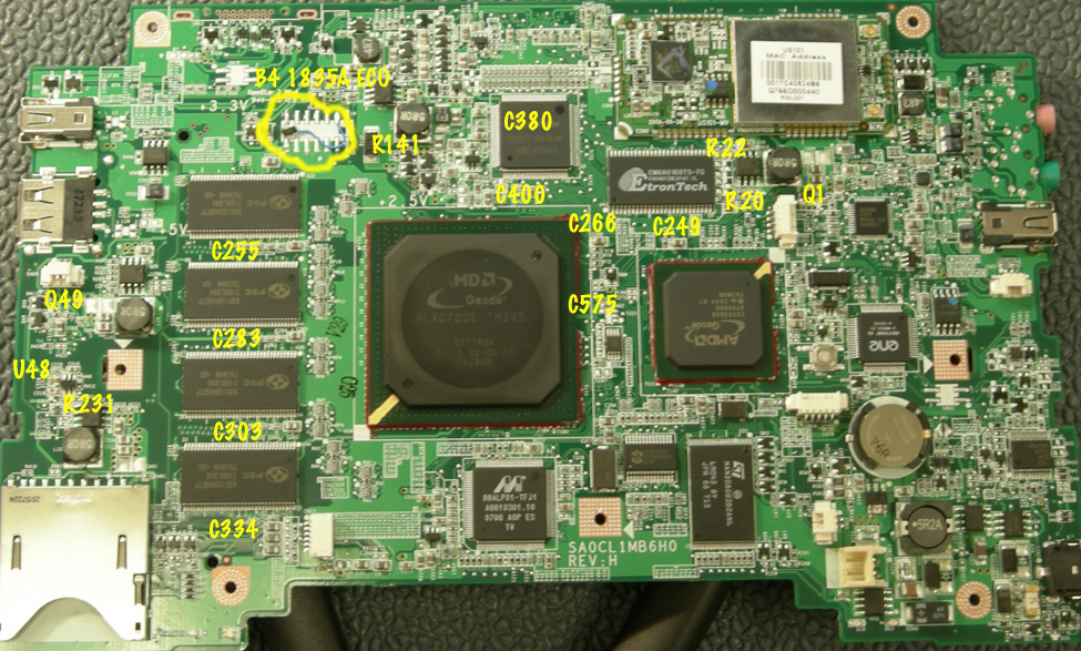
- Modifying the SD Card power switch for soft turn-on, by adding a 0.1 uF, 6.3V capacitor between Q49, pin 2 and ground (available at a pad of an adjacent capacitor).
- Modifying the DCON power switch for soft turn-on, by adding a 4.7 uF, 10V or greater, capacitor across R141.
- Modifying the enable circuitry for the Camera Power switch for staggered turn-on. This consists of removing U48, cutting the trace underneath connecting U48, pins 3 and 4, then soldering U48 (a GMT G9093NHTP1U or a Richtek RT9011-GM) back into place. A 4.7K resistor is then added between pin 3 and pin 4 (conveniently connected to a test pad near pin 3) and a 0.1 uF capacitor is added between pin 3 and ground (available at U48, pin 2).
- Tweaking the compensation of the VMEM power supply by changing R231 to a 33K resistor (SMD0402, 5%).
- Replacing Q1 with a AO3420 (or some other N-channel MOSFET w. an Rds of 25 mOhm or less at a Vgs of 5V). Since the AO3420 is not available in the retail market, I am looking for a suitable alternative for ECOs.
- Adding a 2.2K resistor (10%, SMD0805) across C157. This speeds the discharge of the DCON power supply when it is turned off (allowing quicker turn-on).
- Adding a large number of bypass capacitors. This modification is probably overkill, but some amount of additional bypassing is definitely needed. These additional capacitors (all 0.001uF, X7R) should be located in parallel with the following capacitors (located on the bottom of the board unless otherwise noted):
- SDRAM
- C255, C283, C303, C334 (on top of PCB)
- Southbridge +3.3V supply
- C266, C249, C575 (on top of PCB)
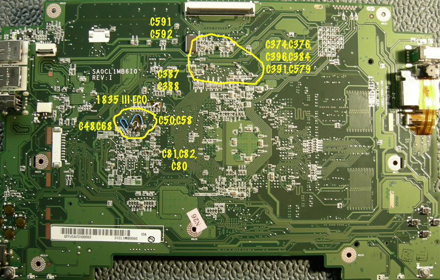
- C48, C50, C58, C68, C80, C81, C82, C391
- WLAN +3.3V supply
- C591, C592
- DCON supplies
- C374, C376, C396, C579
- C387, C388
- C380, C400 (on top of board)
- SDRAM
As this ECR is quite involved, there is a checklist.
Photos
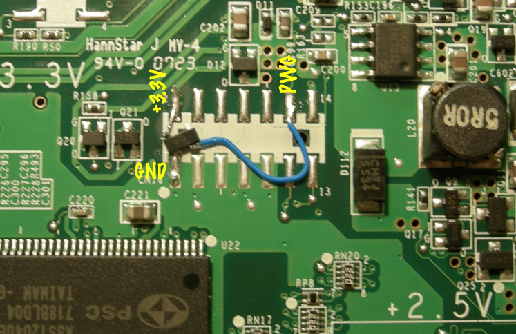
The following photo shows the location of the CPU supervisor (1835 ECO II) on a B4 motherboard, and the location of the other ECR components on the top side of the motherboard. The B4 and C1 build motherboards are almost identical --- all components mentioned in this ECR with the exception of the CPU supervisor are located identically in both builds.
A closeup photo of the CPU supervisor modification on a B4 is also available.
The following photo shows the location of the CPU supervisor (1835 ECO III) on a C1 motherboard, and the location of the other ECR components on the bottom side of the motherboard. A B4 may also be modified placing the CPU supervisor on this side.
Partial Modification
See the warning.
If you only want to do part of this ECR, do all parts except:
- Don't cut the trace underneath U48, or add the 4.7K resistor and 0.1uF capacitor to it. You can mitigate the some of the effects of this by loading a small (22 to 100 uF, 5V or greater) capacitor into location C604 (near R20/U33/Q1).
- Only add the SDRAM bypassing capacitors, as well as the ones parallel to C68, C50, C80, C81, and C81.
Please let us know if you still see Trac ticket #1752 and Trac ticket #1835.
Production Version
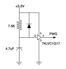
In production, the CPU supervisor used in the ECO of existing machines will be replaced with a cheaper circuit based on an RC circuit and a buffer with hysteresis. This provides a relatively precise delay of the reset signal to the Southbridge, at a reduced cost. If the voltage does temporarily drops below the design specifications, there is a good chance that the system will continue to operate normally.
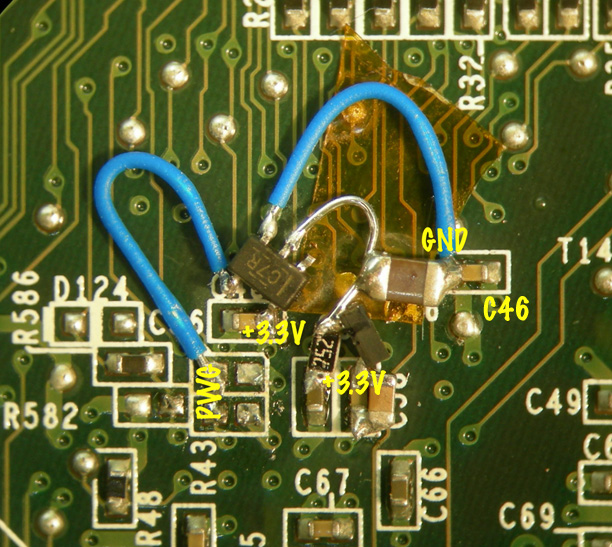
This circuit is included here for reference only, as it is much more difficult to apply to an existing motherboard. Most modified machines use 1835 ECO II instead. In the photo, a 74LVC1G17 in an SC70-5 package is used:
Older Versions
ECO #43
This consists of six parts:
- Tweaking the compensation of the WLAN_3.3V power supply by changing R20 to a 33K resistor (SMD0402, 5%).
- Increasing the voltage of the WLAN_3.3V power supply. There are two common methods:
- Increasing R22 to 32.37K by adding a 768 ohm resistor (SMD0402, 1%) in series to the existing 31.6K resistor
- Decreasing R21 by adding a 330Kohm (SMD0402, 1%) resistor in parallel with the existing 10K resistor
- Allowing the PCI clock time to settle using either:
- variant 43A: Install a 3.10V (3.05 to 3.15V) CPU supervisor, with a delay of at least 16 mS, driving the PWG signal on the motherboard (1835 ECO II), or
- variant 43B: Install an RC circuit and buffer to generate the delay (1835 ECO III).
- Modifying the DCON power switch for soft turn-on, by adding a 4.7 uF, 10V capacitor across R141.
- Modifying the SD Card power switch for soft turn-on, by adding a 0.1 uF, 6.3V capacitor between Q49, pin 2 and ground.
- Modifying the enable circuitry for the Camera Power switch for staggered turn-on. This consists of cutting the trace underneath U48, between pins 3 and 4. A 4.7K resistor is then added between pin 3 and pin 4 (conveniently connected to a test pad near pin 3) and a 0.1 uF capacitor is added between pin 3 and ground (available at U48, pin 2).
The first three of these were described as ECO #42. The remainder are the same on B4 and C1 builds.
ECO #42
This consists of three parts:
- Tweaking the compensation of the WLAN_3.3V power supply by changing R20 to a 33K resistor (SMD0402, 5%).
- Increasing the voltage of the WLAN_3.3V power supply. There are two common methods:
- Increasing R22 to 32.37K by adding a 768 ohm resistor (SMD0402, 1%) in series to the existing 31.6K resistor
- Decreasing R21 by adding a 330Kohm (SMD0402, 1%) resistor in parallel with the existing 10K resistor
- Installing a 3.10V (3.05 to 3.15V) CPU supervisor such as the Micrel MIC811T, with a delay of at least 16 mS, driving the PWG signal on the motherboard
The first two changes are the same for all builds. R20, R21, and R22 are all located right next to U15, the WLAN_3.3V regulator, on the top of the motherboard.
R43 and C56, on the bottom of the motherboard underneath the Southbridge, must be removed.
The third change differs from B4 to C1 builds. On a C1 build machine, the CPU supervisor must be placed on the bottom of the motherboard. See the photos in the final ECR description. On a B4, the CPU supervisor may be installed at the JTAG connector, where all needed signals are conveniently available:
1835 ECO II applied to a B4 motherboard
1835 ECO III
This is both the first test circuitry to verify the significance of clock stability on Trac ticket #1835 (due to the ready availability of the components) and eventually also became the circuit used in production. The difficulty in fabricating this circuit led to most test units having 1835 ECO II applied instead.
C56 and R43 should be removed.
1835 ECO II
The original 1835 ECO had laptops refusing to boot when powered by battery. This eventually led to a more exhaustive study of the laptop power supplies, but initially resulted in a second ECO, using a CPU supervisor with a lower voltage threshold (2.85V - 3.0V), the Micrel MIC811S.
This generally stopped the rebooting problems, but indicated a larger problem --- a significant droop on +3.3V! This was addressed by another part of the ECR, and the CPU supervisors replaced with the Micrel MIC811T (3.05 - 3.15V threshold). On some laptops, the rebooting has continued (Trac ticket #3537) and is the subject of ongoing testing.
C56 and R43 should be removed.
1835 ECO
The original ECO used on a widespread basis to confirm this as a valid fix for Trac ticket #1835 was installing a 3.10V (3.05 to 3.15V) CPU supervisor, with a delay of at least 16 mS between "power good" and deassertion of the Southbridge reset signal (PWG) on the motherboard.
The supervisor used was a MCP130T-315 from Microchip. If this supervisor is used, R43 should remain populated. C56 should be removed. Note that this particular supervisor delays resumes by up to 700 mS!
