XO DC Input Details: Difference between revisions
(→Models) |
|||
| (9 intermediate revisions by the same user not shown) | |||
| Line 7: | Line 7: | ||
===Models=== |
===Models=== |
||
This is a description of the ''original'' DC input power circuit used in the [[Hardware#XO-1.5_Laptop|XO-1.5]] production models ([[XO_1.5_C2|C2]]/[[XO_1.5_C3|C3]]), as well as the ''new'' DC input power circuit introduced with the [[XO_1. |
This is a description of the ''original'' DC input power circuit used in the [[Hardware#XO-1.5_Laptop|XO-1.5]] production models ([[XO_1.5_C2|C2]]/[[XO_1.5_C3|C3]]), as well as the ''new'' DC input power circuit introduced with the [[XO_1.5_C5|C5 production model]]. |
||
The original DC power input circuit (based on a Fujitsu MB39A129) is almost identical to that used in the [[Hardware#XO-1_Laptop|XO-1 laptops]]. The difference was the addition of software control over the input power limit in [[Hardware#XO-1.5_Laptop|1.5]], allowing [[Mppt|MPPT]] algorithms for solar power input. The input protection circuitry was the same. |
The original DC power input circuit (based on a Fujitsu MB39A129) is almost identical to that used in the [[Hardware#XO-1_Laptop|XO-1 laptops]]. The difference was the addition of software control over the input power limit in [[Hardware#XO-1.5_Laptop|1.5]], allowing [[Mppt|MPPT]] algorithms for solar power input. The input protection circuitry was the same. |
||
The battery charge controller used in the ''new'' DC input power circuit (an Intersil ISL9519) is capable of supporting a single battery cell, and operating down to +5V input (although not in the [[XO_1. |
The battery charge controller used in the ''new'' DC input power circuit (an Intersil ISL9519) is capable of supporting a single battery cell, and operating down to +5V input (although not in the [[XO_1.5_C5|XO-1.5 C5]]!) It is planned to continue using it in XO-1.75 (w. two cells) and XO-3. |
||
==Original Circuit== |
==Original Circuit== |
||
| Line 75: | Line 75: | ||
===Existing XO Approach=== |
===Existing XO Approach=== |
||
The approach used in the XO contains two separate sections: |
|||
* F1, D1, and D2 combine to provide functions 3 and 4, and |
|||
* D3, Q1, and the components of the overvoltage protection control provide function 2. |
|||
[[Image:DC_Input_XO-1.png|500px]] |
[[Image:DC_Input_XO-1.png|500px]] |
||
If the voltage exceeds 40V, D1 starts conducting and blows the fuse F1, protecting the motherboard. If the voltage exceeds -40V, D2 blows, followed by F1. |
|||
The DC blocking diode D3 protects against negative input voltages. |
|||
:It is also the only component which prevents battery power from being available at the DC power input --- the body diodes of Q1 and the MOSFET used in the battery charger all conduct when current flows from the battery to the DC power input. |
|||
When the input voltage exceeds 24V, the overvoltage cutoff circuitry stops pulling Q1's gate to ground and it stops conducting (it is a PMOS FET). It provides isolation up to input voltages of 60V, when Q1's max Vds is exceeded. |
|||
The overvoltage cutoff threshold is actually somewhere between 24V and 25V, due to component thresholds, and includes a turn-on hysteresis (the voltage must drop several hundred millivolts below the turn-off voltage before Q1 will be turned back on). It is guaranteed to be above 24V, to accommodate common solar cells, and is typically 24.5V. |
|||
===Improvements=== |
===Improvements=== |
||
The biggest problem with the existing XO DC input protection circuitry is that it isn't very good at #1. Diode D1 presents a 0.4V voltage drop, which can waste up to 0.8W when initially charging a fully dicharged battery. One proposal is to replace D1 with another PMOS FET: |
|||
[[Image:DC_Input_propA.png|500px]] |
[[Image:DC_Input_propA.png|500px]] |
||
====Undervoltage Control Circuit==== |
|||
This leaves us with the question of what the Undervoltage Cutoff circuit should be. |
|||
The simplest approach would be just to tie the gate to ground: |
|||
[[Image:DC_Input_propB.png|300px]] |
[[Image:DC_Input_propB.png|300px]] |
||
This minimalist approach does turn off Q1 when the input voltage is negative, but only if there is no voltage present on the system side. In the XO-1/1.5, where the battery voltage provides a constant 5.5 to 6.5V on the system side, Q1 is constantly on. |
|||
| ⚫ | |||
A somewhat better approach is shown below. In this circuit, R1 keeps Q1 turned on, unless Q2 is turned on. Q2 is kept turned on whenever the voltage at node B is greater than the voltage on node A, making the dubious assumption that the Vf of D1 and Vbe of Q2 are similar. R2 is provided to ensure that the maximum Vgs of Q1 is not exceeded when passing up to 40V. |
|||
There are, however, numerous problems remaining with this circuit: |
|||
* It relies on somewhat of a match between D1 and Q2. It is unclear how this will perform across temperature. |
|||
:One version of this design uses the base/emitter junction of a matched transistor instead of D1. The problem is that most base/emitter junctions are only rated for 5 or 6V of reverse voltage before failing. |
|||
* It still fails in that once the circuit is turned on, it won't turn off until there is a significant voltage difference between the input and output. |
|||
:Philosophically, I'm not sure there is a solution. Ideally, the circuit doesn't turn on until there is a voltage difference, but keeps this voltage difference to a minimum (as it represents the power loss). In practice, this circuit sees a voltage drop of 40 to 70 mV across Q1 (at up to 2A). |
|||
| ⚫ | |||
An improved version of this is: |
|||
[[Image:PropC_UVP.png|400px]] |
|||
In this circuit, the forward voltage drops are matched, with diodes providing protection against negative voltage and a transistor providing switching of the main switch. R4 is provided to ensure that the reverse voltage seen by Q3 doesn't exceed 5V when the input is at -40V. R5 is provided simply for circuit symmetry. |
|||
Latest revision as of 00:52, 3 May 2011
This page describes the XO DC Input circuit (requirements) in detail.
Introduction
The DC power input circuit on the XO laptop is unique. It is designed to accept a power from a wide range of input voltages (11 to 24V), protect itself from harm by a larger range of input voltages (-40 to 40V), and is also designed to seek the maximum power point of a solar input device.
Models
This is a description of the original DC input power circuit used in the XO-1.5 production models (C2/C3), as well as the new DC input power circuit introduced with the C5 production model.
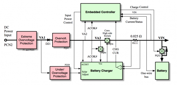
The original DC power input circuit (based on a Fujitsu MB39A129) is almost identical to that used in the XO-1 laptops. The difference was the addition of software control over the input power limit in 1.5, allowing MPPT algorithms for solar power input. The input protection circuitry was the same.
The battery charge controller used in the new DC input power circuit (an Intersil ISL9519) is capable of supporting a single battery cell, and operating down to +5V input (although not in the XO-1.5 C5!) It is planned to continue using it in XO-1.75 (w. two cells) and XO-3.
Original Circuit
The original circuit provides the MPPT algorithm running on the Embedded Controller the following values:
- Input Voltage (VA2)
- Output Current from the battery charger, which is the sum of the system current and the battery current
- Output Voltage (VIN), equivalent to the battery voltage.
- Battery Voltage and Current, obtained via one-wire from the battery gas gauge
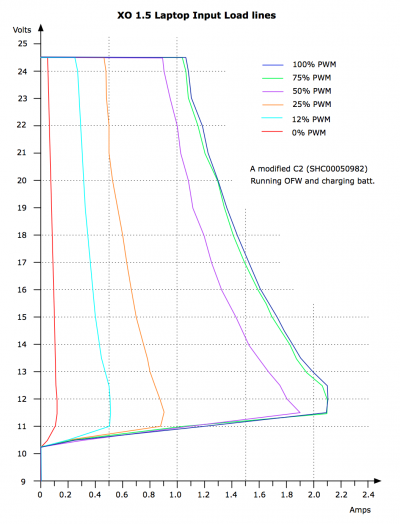
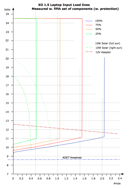
Hardware imposes a shape on the DC input impedance as shown in the following diagram. In particular, a maximum input power is specified (not a maximum input current) and the maximum input power decreases drastically as the input voltage drops below 11V.
The maximum input power may be modified under software control as shown by the 25%, 50%, and 75% curves. The precision varies but roughly 32 power steps are available.
Squeal
In order to operate with solar cells, the original circuit on XO-1 had a circuit that, starting a particular voltage, quickly cut the current input by the laptop back to zero. This means that even if a solar cell is undersized and underlit, it might provide a few milliwatts at 10.5V (with MPPT, we dynamically change the impedance to get more milliwatts at 14-16V). The particular voltage at which this circuit triggers and drops the current is set by a pair of resistors, a voltage source in the charger IC, and the parameters of a transistor. This current drop is seen at the bottom of the above input impedance graph for an XO-1.5 C3 laptop.
Key to the operation of this circuit (and preventing oscillation) is that the DC charger detect DC input and operate to a voltage below that at which the charger stops accepting current from the input. It is on, but we are telling it to supply no current to the laptop. This is set by a separate pair of resistors, and a separate voltage threshold in the charger.
Fast forward part of a year, and a completely new hardware team was finishing up testing when they realize that the laptop powers itself off if the battery is low and a DC adapter is plugged in (#2182). The fix seems innocuous, but it inadvertently added a 0.35V difference between the "DC input voltage" sensed by the two circuits (and in the wrong direction). This greatly increased the probability of oscillation when using solar cells.
The solution to both problems is to spread the two voltage thresholds farther apart. This was tested on real hardware today, and it does eliminate any squealing when the laptop is powered by a completely under-powered/under-illuminated solar panel. At the same time, it is possible for the EC firmware to detect this squeal (rapid turn-on/off of the battery charger) and use it as an indicator that input power needs to be reduced. Due to the next problem (voltage drop on the EC voltage sense), it turns out to be the most reliable way of detecting this condition!
Voltage Drop
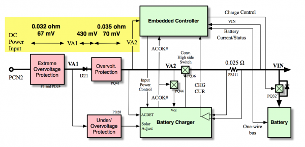
A critical flaw in the design has finally been identified. The input voltage sensed by the EC is sensitive to the power drawn by the system --- up to 0.55 V of drop occurs as the input current increases from 0 to 2A ! The net effect of this is that voltages measured by the EC at the DC input are not accurate for use in an MPPT algorithm.
New Circuit
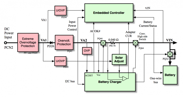
A new battery charger circuit was phased into production in the spring of 2011. This circuit provides the MPPT algorithm running on the Embedded_controller the following values:
- Input Voltage (VA1)
- Input Current to the battery charger
- Output Voltage (VIN), equivalent to the battery voltage.
- Battery Voltage and Current, obtained via one-wire from the battery gas gauge
The new battery charger (an Intersil ISL9519) requires additional circuitry to decrease the maximum input power as the input voltage drops below 11V. It was decided to attempt to control the maximum input power at higher input voltages through EC firmware. That is not shown in the following input impedance diagram:
Input Protection
The input protection circuit has four functions:
- When the voltage of the external power source is within the operating range of the laptop (9-24V), power should be transmitted with minimal loss to the battery charger.
- In the event of input voltages outside of the operating range, the laptop motherboard is disconnected from the external power source. The connection is restored when the applied voltage returns to an acceptable voltage.
- In the event of egregious input voltages (less than -40V or greater than 40V), the laptop motherboard is permanently disconnected from the external power source. After such an overvoltage, up to three components on the motherboard may need repair, but outside of protective circuitry (fuse and diodes) the motherboard should be unharmed.
- In the event of catastrophic failure of the motherboard, it prevents an excess of current from being drawn from an external power source. Repair of the motherboard will be needed.
Simple Approach
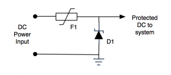
The simplest approach uses a resettable fuse (polyfuse), F1, with a zener diode, D1, tripping the fuse in the case of negative voltage or overvoltage.
The problem with this approach is that surface-mountable resettable fuse technology does not work well at higher temperatures and currents.
Existing XO Approach
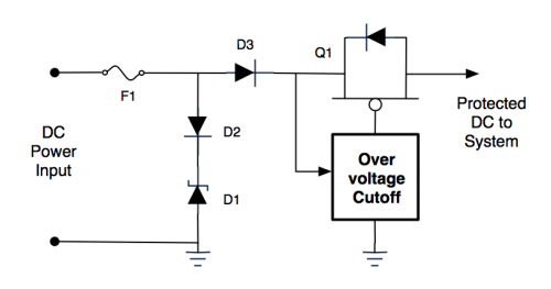
The approach used in the XO contains two separate sections:
- F1, D1, and D2 combine to provide functions 3 and 4, and
- D3, Q1, and the components of the overvoltage protection control provide function 2.
If the voltage exceeds 40V, D1 starts conducting and blows the fuse F1, protecting the motherboard. If the voltage exceeds -40V, D2 blows, followed by F1.
The DC blocking diode D3 protects against negative input voltages.
- It is also the only component which prevents battery power from being available at the DC power input --- the body diodes of Q1 and the MOSFET used in the battery charger all conduct when current flows from the battery to the DC power input.
When the input voltage exceeds 24V, the overvoltage cutoff circuitry stops pulling Q1's gate to ground and it stops conducting (it is a PMOS FET). It provides isolation up to input voltages of 60V, when Q1's max Vds is exceeded.
The overvoltage cutoff threshold is actually somewhere between 24V and 25V, due to component thresholds, and includes a turn-on hysteresis (the voltage must drop several hundred millivolts below the turn-off voltage before Q1 will be turned back on). It is guaranteed to be above 24V, to accommodate common solar cells, and is typically 24.5V.
Improvements
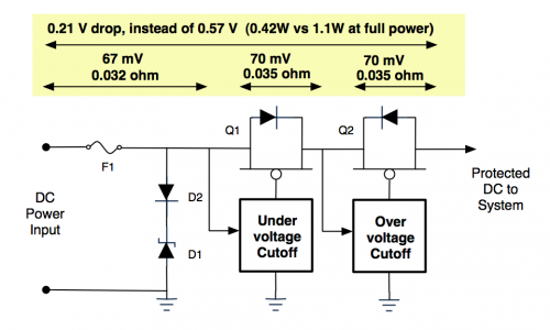
The biggest problem with the existing XO DC input protection circuitry is that it isn't very good at #1. Diode D1 presents a 0.4V voltage drop, which can waste up to 0.8W when initially charging a fully dicharged battery. One proposal is to replace D1 with another PMOS FET:
Undervoltage Control Circuit
This leaves us with the question of what the Undervoltage Cutoff circuit should be.
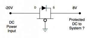
The simplest approach would be just to tie the gate to ground:
This minimalist approach does turn off Q1 when the input voltage is negative, but only if there is no voltage present on the system side. In the XO-1/1.5, where the battery voltage provides a constant 5.5 to 6.5V on the system side, Q1 is constantly on.
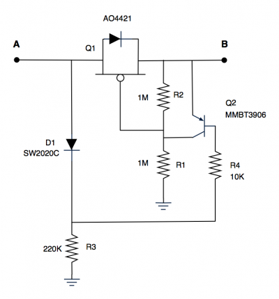
A somewhat better approach is shown below. In this circuit, R1 keeps Q1 turned on, unless Q2 is turned on. Q2 is kept turned on whenever the voltage at node B is greater than the voltage on node A, making the dubious assumption that the Vf of D1 and Vbe of Q2 are similar. R2 is provided to ensure that the maximum Vgs of Q1 is not exceeded when passing up to 40V.
There are, however, numerous problems remaining with this circuit:
- It relies on somewhat of a match between D1 and Q2. It is unclear how this will perform across temperature.
- One version of this design uses the base/emitter junction of a matched transistor instead of D1. The problem is that most base/emitter junctions are only rated for 5 or 6V of reverse voltage before failing.
- It still fails in that once the circuit is turned on, it won't turn off until there is a significant voltage difference between the input and output.
- Philosophically, I'm not sure there is a solution. Ideally, the circuit doesn't turn on until there is a voltage difference, but keeps this voltage difference to a minimum (as it represents the power loss). In practice, this circuit sees a voltage drop of 40 to 70 mV across Q1 (at up to 2A).
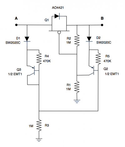
An improved version of this is:
In this circuit, the forward voltage drops are matched, with diodes providing protection against negative voltage and a transistor providing switching of the main switch. R4 is provided to ensure that the reverse voltage seen by Q3 doesn't exceed 5V when the input is at -40V. R5 is provided simply for circuit symmetry.
